Electric heating vacuum annealing furnace for semiconductor annealing
 11-12-2025 Author: KJ technology
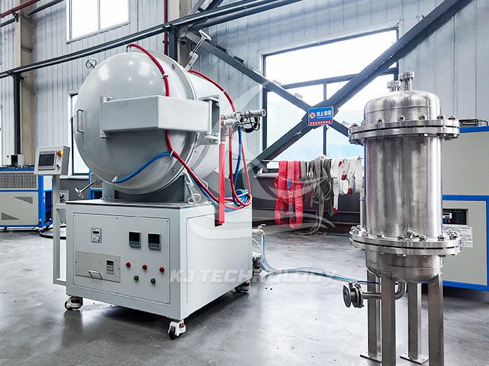
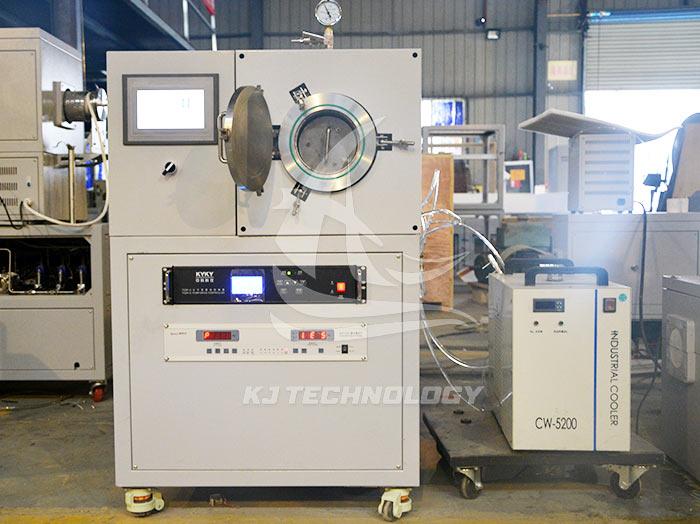
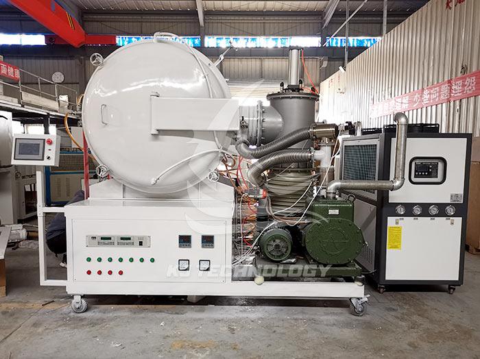
Electric heating vacuum annealing furnace has significant advantages in semiconductor annealing treatment, which can improve the performance and reliability of semiconductor materials through vacuum environment and precise temperature control technology. The following is a specific explanation:
1. Core advantages
Vacuum environment inhibits oxidation
The vacuum annealing furnace isolates oxygen through a high vacuum system (with a maximum vacuum degree of 1 × 10⁻³Pa or even lower) to prevent semiconductor materials from reacting with oxygen, water vapor, and other substances at high temperatures, thereby preventing surface oxidation and contamination. For example, in silicon wafer annealing, a vacuum environment can reduce the formation of oxide layers, maintain surface smoothness, and improve device yield.
Accurate temperature control ensures performance
By using PID closed-loop control technology, temperature fluctuations can be controlled within a very small range (such as ± 0.75 ∘ C), ensuring uniform and stable temperature of semiconductor materials during annealing. This high-precision temperature control is crucial for activating doped atoms and repairing crystal defects. For example, in the back-end process of CMOS devices, rapid annealing can reduce oxide trap charges and interface state density, improving device reliability.
Rapid temperature rise and fall to improve efficiency
Equipped with efficient heating elements (such as resistance wires, induction heating) and a rapid cooling system, the heating rate can reach 150 ∘ C/s, and the cooling rate is also significant. Rapid Heat Treatment (RTP) technology can shorten the process cycle and avoid thermal damage to materials due to prolonged exposure to high temperatures, making it suitable for large-scale production.
2. Typical application scenarios
Wafer Annealing and Doping Activation
Stress relief: In the manufacturing process of silicon wafers, annealing can eliminate internal stresses generated by mechanical processing or ion implantation, and improve the quality of crystal crystallization.
Doping process: By controlling the annealing temperature and time, the diffusion and activation of doped atoms (such as boron and phosphorus) are achieved, optimizing the electrical properties of semiconductors. For example, in the annealing of power semiconductor SiC materials, high-temperature treatment can reduce defect density, improve breakdown voltage and carrier mobility.
Thin film growth and repair
Preparation of GaN thin film: Vacuum annealing can improve the crystalline quality of the film, reduce stress, and enhance optoelectronic performance.
After polishing repair: Rapid annealing can eliminate surface damage caused by chemical mechanical polishing (CMP), reduce roughness, and enhance device stability.
Optimization of packaging process
Wire bonding: Annealing can eliminate internal stresses generated during wire cutting and assembly processes, improving packaging reliability.
Metal deposition post-treatment: Crystallize deposited metals (such as aluminum and copper) to improve electron transport capability and reduce contact resistance.
3. Technical parameters and equipment selection
key parameters
Vacuum degree: Depending on the sensitivity of the material, it is generally required to be 0.1-1Pa, and high-end equipment can reach 1 × 10⁻⁴Pa.
Temperature range: usually covering 130 ° C to 1200 ° C, meeting different material requirements.
Heating and cooling rate: The rapid annealing furnace needs to support adjustable temperatures of 5-20 ° C/minute, or even higher.
Temperature uniformity: The temperature difference within the effective heating zone should be controlled within ± 3 ° C.
Equipment selection suggestions
Laboratory level: Choose a desktop vacuum RTP rapid annealing furnace with high-precision temperature control, fast lifting and cooling, and compact design, suitable for material research and development and small batch production.
Industrial grade: Priority is given to large vacuum annealing furnaces, which support multi-stage programming and special gas environments such as hydrogen to meet the needs of large-scale production.
4. Industry Cases
In the military industry, a certain research institute requires a vacuum degree of 10-4Pa for 24 hours to achieve precision device oxidation free annealing through a vacuum annealing furnace, ensuring stable performance.
Power Semiconductor: A certain enterprise uses hydrogen annealing technology to process SiC materials, and through the support of 50 program programming in the Zhongke Comrade vacuum annealing furnace, completes 120 hours of continuous annealing, breaking through the process bottleneck.


